
Characterization of SPR and Waveguide Structures for Sensor Applications
The Model 2010/M is an ideal tool for developing surface plasmon resonance (SPR) and waveguide structures for use as bio- or other sensors. Such sensor devices usually rely on measuring the angular shift of an SPR resonance or waveguide propagation mode caused by the adsorption of thin layers of target materials on the surface of the sensor.
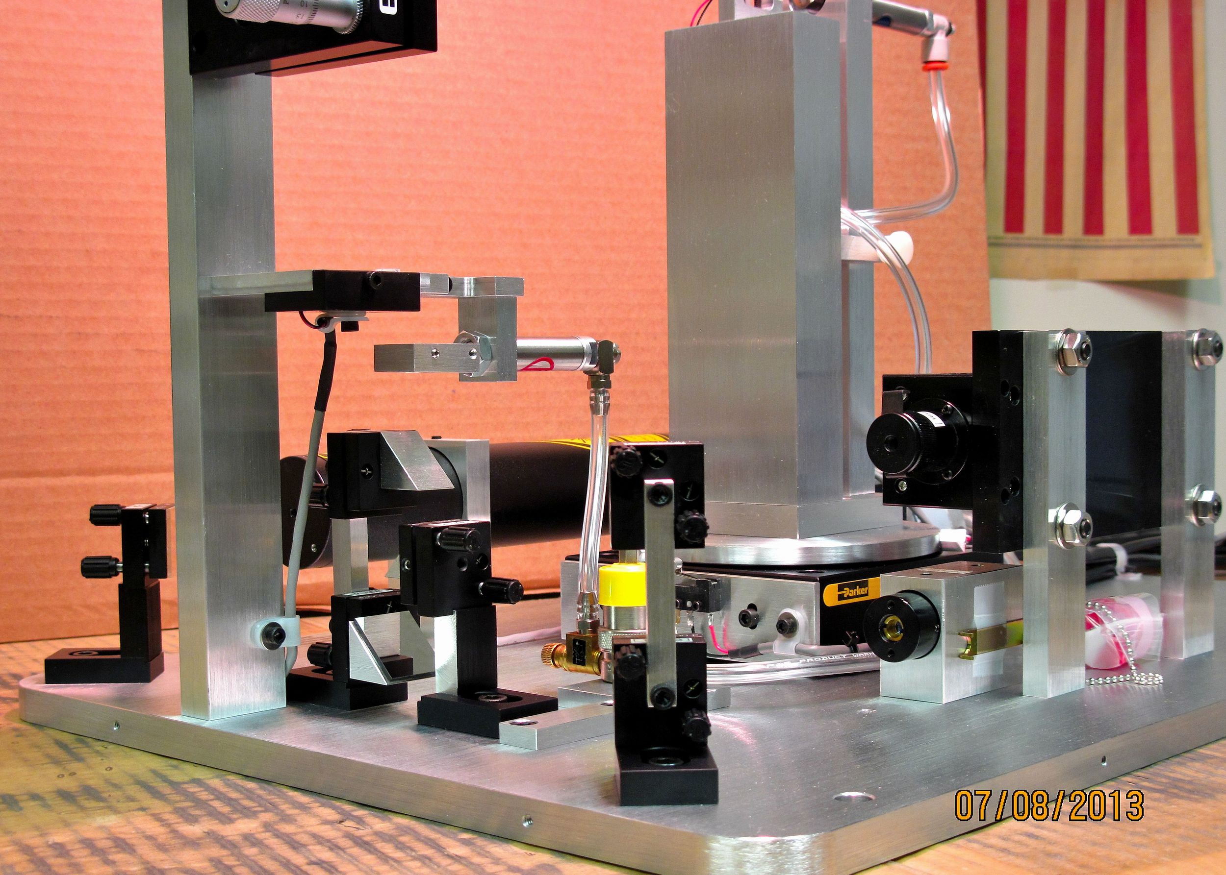
A typical SPR sensor structure consists of a glass slide covered on one side with a thin layer of gold or silver. Kretschmann-type SPR measurements are easily performed on the Model 2010/M using the technique described by Kotchev et al (Colloid Polym. Sci. vol 281 (2003), 343-352). In this method, a small drop of index matching oil is placed on the surface of the 2010/M measuring prism to make contact to the uncoated side of the SPR sensor device (figure 1):

The 2010/M’s computer-driven rotary table varies the incident angle, and a sharp dip in the light reflected from the glass/metal film interface, caused by the SPR resonance, occurs (curve 1 in Figure 2). The SPR resonance angle depends on the laser wavelength and the metal film thickness and type, but the angle is also strongly affected by the presence of even extremely thin layers (1-10 nm) present on the metal surface (curve 2 in figure 2). This extreme sensitivity of the resonance angle to both the thickness and the refractive index of thin adsorbed layers makes the SPR structure an ideal sensor for both organic/biological and inorganic material types at the nanolayer level.
Since SPR resonances often occur at effective indices below the normal range of most Metricon prisms, special index matched prisms are available for SPR applications on the 2010/M. In addition, it is usually easy to accommodate SPR devices which incorporate fluidic apparatus to allow liquids to come into contact with the SPR sensor – if we know in advance the design of your cell and other special requirements, we can usually customize the 2010/M system to suit your needs at little or no additional cost.
Waveguide sensors work in a roughly similar way to SPR sensors and usually rely on the angular shift induced in mode propagation angles caused by thin adsorbed layers of the target molecules on the waveguide surface (see Bahsi et al, Sensors, vol. 9 (2009), 4890-4900). Detection of very low levels of DNA molecules has also been demonstrated by absorption into porous silicon waveguides (Rong et al, Appl. Phys. Lett., vol. 93 (2008), 161109).
The following is a partial list of journal articles referencing Metricon equipment for biosensor applications:
M-L Anne , J. Keirsse , V. Nazabal , K. Hyodo, S. Inoue, C. Boussard-Pledel, H Lhermite, J. Charrier, K. Yanakata, O. Loreal, J. Le Person, F. Colas, C. Compère and B. Bureau, “Chalcogenide Glass Optical Waveguides for Infrared Biosensing”, Sensors, vol. 9(9) (2009), pages 7398-7411.
Z.B. Bah_i, A. Büyükaksoy, S.M. Ölmezcan, F. _im_ek, M.H. Aslan, A.Y. Oral, “A Novel Label-Free Optical Biosensor Using Synthetic Oligonucleotides fromE. coli O157:H7: Elementary Sensitivity Tests”, Sensors, vol. 9 (2009) pages 4890-4900.
S. Grego, J. R. McDaniel, and B. R. Stoner, “Wavelength interrogation of grating-based optical biosensors in the input coupler configuration”, Sensors and Actuators B: Chemical, vol. 131, Issue 2, 14 May 2008, pages 347-355.
Y. Jiao and S. M. Weiss, “Design parameters and sensitivity analysis of polymer-cladded porous silicon waveguides for small molecule detection”, Biosensors and Bioelectronics, vol. 25 Issue 6, 15 February 2010, pages 1535-1538.
D. Lloyd, L. Hornak, S. Pathak, D. Morton, and I. Stevenson, “SPARROW: A New Thin Film Based Biosensor Chip Technology,” Vacuum Technology & Coating, September 2004, pages 48-57.
A. K. Manocchi , P. Domachuk, F. G. Omenetto, H. Yi, “Facile fabrication of gelatin-based biopolymeric optical waveguides”, Biotechnology and Bioengineering, vol. 103, No. 4, July 1, 2009, pages 725-732.
M. Nordstrom, D. A. Zauner, A. Boisen, J. Hubner, “Single-Mode Waveguides With SU-8 Polymer Core and Cladding for MOEMS Applications”, J. Lightwave Tech., vol. 25, issue 5 (2007) pages 1284-1289.
S. T. Parker, P. Domachuk, J. Amsden , J. Bressner , J. A. Lewis, D. L. Kaplan, F. G. Omenetto, ” Biocompatible Silk Printed Optical Waveguides”, Adv. Materials, vol. 21, Issue 23, pages 2411-2415
G. Rong, J. D. Ryckman, R. L. Mernaugh, and S. M. Weiss, “Label-free porous silicon membrane waveguide for DNA sensing”, Appl. Phys. Lett., 93, 161109. (2008).
G. Rong, A. Najmaie, J. E. Sipe, S. M. Weiss, “Nanoscale porous silicon waveguide for label-free DNA sensing”, Biosensors and Bioelectronics, Vol. 23, Issue 10, 15 May 2008, Pages 1572-1576.
A. Samoc, A. Miniewicz, M. Samoc, J. G. Grote, “Refractive-Index Anisotropy and Optical Dispersion in Films of Deoxyribonucleic Acid”, J. Appl. Pol. Sci., vol. 105, 236-245 (2007).
B.Y. Shew, C.H. Kuo, Y.C. Huang, Y.H. Tsai , “UV-LIGA interferometer biosensor based on the SU-8 optical waveguide”, Sensors and Actuators A: Physical, Vol. 120, Issue 2, 17 May 2005, Pages 383-389.
L. D. Williams, M. Okandon, and S. Blair, “Design and characterization of a microheater array device fabricated with SwIFT-LiteTM”, J. Micro/Nanolith. MEMS MOEMS Vol. 7, 043035 (Nov. 10, 2008).